Recent demands from hospitals, practitioners, and even patients themselves calling for more functions and increased portability, has created a market for upgraded surgical, diagnosis, and monitoring equipment. Coupled with increasing medical costs, the push for shorter hospital stays has increased the need for upgraded portable monitoring equipment that can physically travel with the patient through recovery and after release. As a result of this dynamic change in the medical service system, a new focus has been driven towards smaller, lighter, and more portable medical equipment. In order to accomplish this, every portion of the medical device itself is considered a candidate for miniaturization.
Big Changes, Smaller Sizes

Fortunately for medical designers, earlier models from other industries were able to lay the foundation towards the evolution of miniaturization within the medical device market. Cell phones, laptop computers, and digital cameras, among others, all contained high-performing chip technology that served a growing demand and a growing appetite for more functions—at half the size. Thankfully, one of the key elements emerged within the new semiconductor technology called the complementary metal-oxide semiconductor (CMOS) technique.
This technique, in particular, has allowed a significant increase in function and processing capacity, simultaneously increasing the density while, at the same time, physically reducing the size and weight. In fact, some of the earliest adopters in the medical field striving for miniaturization included pacemaker manufacturers. These manufacturers used the newfound semiconductor technology to combine both analog and digital signals into a single-chip pacemaker.
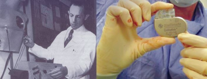
In turn, designers were now able to reduce the physical size and weight of this patient-worn device, while improving overall patient comfort, as well as increasing the physical analysis and control functions of the pacemaker. Hard to believe that a design once the size of a microwave oven, evolved into the footprint of a silver dollar. (See Figure 1)
Advancements in displays, storage, and microprocessors also contributed to miniaturization. Like semiconductors, new feature-rich displays were fitting more complex controls into a single chip, thereby reducing board area and improving visibility. Storage technology also became increasingly compact, particularly the availability of small form factor flash storage devices now available, such as micro SD cards.
Soon thereafter, other instruments from stethoscopes to laparoscopic cameras all followed suit using similar chip techniques beginning a miniaturization metamorphosis of sorts. This has been one of the key elements aiding in the ability to make portable medical devices more of a reality and it’s these smaller, smarter electronics leading the way for breakthroughs like minimally invasive surgery (MIS).
MIS unlike traditional methods, avoids cutting into muscle altogether. In fact, more and more MIS procedures are being conducted utilizing robotic technology, such as the Da Vinci surgical system. This enables procedures, such as a hysterectomy, to be completed through only a few small holes in the abdomen. When performed robotically, the surgery, on average, requires only one day of hospital recovery as opposed to three to four days with conventional methods. Patients come away with limited scarring, very little pain, and far less blood loss. Perhaps best of all, patients can return to their regular lifestyle much faster. Rapid changes in technology are making this possible.
Devices including laparoscopic cameras and camera capsules have given surgeons a clear view of the surgical field even when using a smaller diameter scope. This, in turn, translates into smaller incisions and reduced pain. Recent upgrades to this as well has now enabled high-definition viewing to provide wide-angle views, allowing surgeons to quickly identify instruments moving in and out of the surgical field.
Now, whether it’s pacemakers, cameras, probes, sensors, and more, these mini-medical systems on a single chip have quite frankly changed the rules and electrical demands within the whole instrument, paving the way for smaller electronics to be born. Older electronic circuits using analog technology required relatively high voltage and consumed considerably more electrical current. Upfront, these instrument boxes began with large power supplies consisting of bulky wiring systems running circuitry throughout the entire instrument, all essential to feed the electricity-hungry modules inside. Meanwhile, the wires themselves had to be large enough to handle the current flow. Couple these factors together and they created an enormous design challenge for developers striving for miniaturization.
The Push Forward

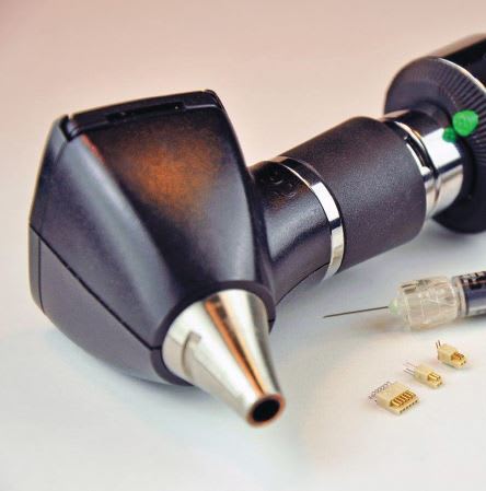
These days, however, the quest for miniaturization is a little more realistic. Medical chips no longer require the same level of support and protection, as these signals are predominately digital. Voltages are usually regulated from 12 volts down to as low as 3 volts while the physical current flow on average dropped from nearly 3 amps per, to the 100 milliamp range, if not lower. Even the power supplies themselves are dramatically becoming smaller and lighter in weight, making miniaturization more of a realization than ever before. (See Figure 2)
It is this so called “changing of the guard” that’s enabling the instruments themselves to become smaller while, at the same time, significantly reducing the size of electrical components within, such as connectors and wiring harnesses. As a result, micro and nano-miniature connectors began to enter the scene. These smaller connectors were able to solve additional size and reliability problems that had plagued medical device designers for years.
Designers found that by using these miniature connectors not only did they see an increase in reliability, but they also witnessed increases in general ruggedness and overall product life. That is, “IF” medical designers were willing to embrace these new high reliability standards previously proven to work by other high-technology applications, such as military and aerospace.
Cable and connector manufacturers addressing this marked transformation have developed miniature connector families specifically for the medical industry. Using wiring made up of 26 to 34 AWG conductors (or smaller), these custom medical cables became more flexible and capable of holding more signals with half the size and weight of previous interconnect solutions. Connector manufacturers, in particular, have aided in reducing the overall size of these older D-Sub type connectors (100 mil. Pitch) often found within household computers and printers, and replaced them with new technology with half (.50"/1.3mm Pitch) or even one quarter (.025"/ .625mm Pitch) the footprint.

Now as the evolution of miniaturization continues to challenge medical equipment designers, two factors still stand head and shoulders above the rest: quality and reliability. Companies like Omnetics Connector Corporation select the highest reliability elements for use within medical assemblies. The spring pin and socket contact system has proven reliability over wide ranges of shock, vibration, and thermal changes. Made of beryllium copper with high tensile strength, it manages to withstand the rigors of use and abuse often experienced in the hurried business of patient service. These same pin and socket elements selected also pass plating tests specified in Mil. B488-type II, Code C class 1.27. This requires a strong nickel plate barrier that is then coated with 50 micro-inches of gold.
When placed into miniature insulator housings, molded from liquid crystal polymer (LCP) or polyphenylene sulfide (PPS), the connector remains at the highest level of reliability testing in medical, military, and aerospace industries. These miniature assemblies often consist of Teflon® insulated wiring that is carefully laser stripped to avoid nicking the miniature wiring inside. Individual wires are then crimped into the back section of the contact system. The pin-and-wire set is then inserted into the LCP/PPS insulator and fixed in place with an epoxy. An over-molded shell or strain relief can be customized to the designer’s criteria to complete a more aesthetically pleasing and/or user friendly assembly. (See Figure 3) If a more rugged solution is needed, the loaded insulator can be inserted into a metal housing to finalize the miniature medical connector.
The benefits of this assembly process include precision, very tight tolerances, and, above all, high quality miniaturization that greatly exceeds the performance of single spade pins in lower quality plastic housings. These micro and nanominiature connectors can now be integrated into the design of medical instruments during the early design stages though the use of solid models. These same connector solid model designs can be directly interfaced on-line by equipment designers to adjust shells and/or insulators to fit directly into handles, probes or even custom mounted into instruments. The design characteristics allow for an overall better fit and use of instrument in many design forms.
These new miniaturized connectors match up perfectly with the evolution of medical electronics. They support instrument portability as well as the push for size reduction in medical devices, while retaining the highest reliability standards we all expect for our own medical services. Through various opportunities within the medical industry, new connector and cable designs have helped solve miniaturization challenges by providing new methods for addressing data-acquisition, sample collection, portability, and more through the use of simple, comfortable, affordable miniature cable systems.
This article was written by Derek Hunt, Applications Specialist, Omnetics Connector Corporation, Minneapolis, MN. For more info rmation, visit http://info.hotims.com/45607-167 .


